Overview
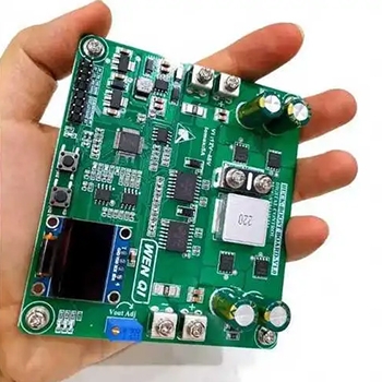
As a key electronic component, a DC-DC converter is responsible for voltage conversion between direct current (DC) power sources. Its core function lies in efficiently achieving voltage step-up and step-down, polarity inversion, and power isolation. In particular, Powerhome converters feature a variety of characteristics such as high efficiency, high reliability, low noise, and ease of integration, making them indispensable in a wide range of electronic devices.
1. Key Features
A DC-DC converter, as a critical element in DC circuits, primarily converts electrical energy from one voltage level to another with high efficiency. By performing voltage conversion between DC power supplies, the converter ensures efficient power transfer and demonstrates advantages such as efficiency and reliability, which enable its widespread use in electronic equipment. For example, a converter can easily transform a 5.0V DC input into either 1.5V or 12.0V DC output. Such a device is referred to as a DC-DC converter and is sometimes also called a switching power supply or a switching regulator.
These converters are typically composed of a control chip, an inductor coil, diodes, transistors, and capacitors. When evaluating the performance of a DC-DC converter, focusing solely on the control chip is insufficient. In fact, the characteristics of peripheral circuit components and the layout of the circuit board also significantly affect the performance of the power supply. Therefore, a comprehensive assessment must be conducted.
2. Applications
DC-DC converters are widely used, not only simplifying the design of power circuits and shortening the development cycle, but also optimizing various performance indicators. Capable of meeting different voltage requirements, DC-DC converters streamline power design, enhance efficiency, and play a vital role across multiple sectors. They are extensively applied in power electronics, military systems, scientific research, industrial control equipment, and communication devices, and they also serve an essential role in advanced fields such as automotive electronics and aerospace.
Moreover, consumer electronics such as mobile phones, MP3 players, digital cameras, and portable media players also rely heavily on DC-DC converters. From a circuit perspective, DC-DC converters belong to a type of chopper circuit.
Working Principle
1. Modulation Methods
In DC-DC converters, PFM and PWM are two important modulation techniques. PFM (Pulse Frequency Modulation) maintains a constant switching pulse width and stabilizes the output voltage by adjusting the frequency of the output pulses. PWM (Pulse Width Modulation), on the other hand, controls the stability of the output voltage by varying the pulse width. Both PFM and PWM serve as primary modulation methods in DC-DC converters, providing optimal energy efficiency under different load conditions. This type of control is particularly effective under light-load scenarios, significantly reducing power consumption and ensuring long-term economic operation.
2. Common Architectures
DC-DC converters exhibit several notable characteristics, with common architectures including Buck, Boost, and Buck-Boost converters. These three main topologies are suited to different voltage conversion requirements, each with its own advantages and limitations.
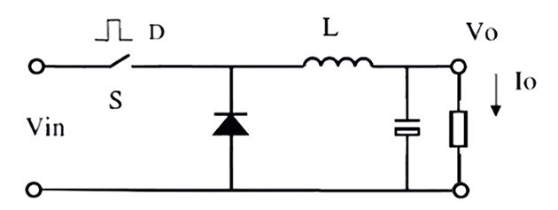
Buck (Step-Down DC/DC Converter): A Buck converter is a step-down DC/DC converter. Its core principle lies in adjusting the on and off times of the switching transistor to regulate the output voltage level. This type of converter is widely used in various electronic devices and is favored for its simplicity and high conversion efficiency.
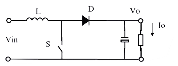
Boost (Step-Up DC/DC Converter): A Boost converter is a step-up DC/DC converter, and its operating principle is the opposite of that of a Buck converter. By adjusting the on and off times of the switching transistor, it increases the input voltage to achieve the desired higher output voltage. This type of converter is widely used in applications that require elevated voltage levels, such as electric vehicle charging systems and photovoltaic (solar power) generation systems.
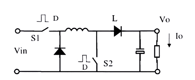
Buck-Boost (Step-Up/Step-Down DC/DC Converter): A Buck-Boost converter is a type of DC/DC converter capable of both stepping down and stepping up the input voltage. Its operating principle is unique, as it regulates the input voltage by adjusting the on and off times of the switching transistor, thereby achieving either step-down or step-up conversion. This converter performs exceptionally well in applications where the power supply voltage has a wide range or where flexible voltage adjustment is required, such as in portable electronic devices and aerospace systems.
Key Points in DC-DC Circuit Design
Component Selection and Peripheral Design
In DC-DC circuit design, it is essential to select appropriate components and peripheral elements such as capacitors, inductors, and resistors to ensure requirements for performance, ripple, efficiency, and safety are met. Among these, the continuous output current capability of the selected components is a critical parameter. This specification must be carefully considered, and sufficient margin should be reserved. At the same time, factors such as instantaneous peak current and heat generation of the circuit must also be comprehensively evaluated to meet derating requirements and ensure reliable operation.
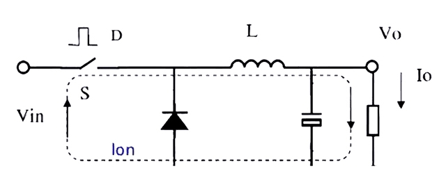
When evaluating power supply performance, efficiency is an important consideration. It is necessary to examine efficiency under both light-load and heavy-load conditions. Under light-load conditions, efficiency directly affects the standby power consumption of the supply, while under heavy-load conditions, efficiency is closely related to temperature rise. Typically, particular attention is paid to the efficiency at 12V input and 5V output under a 10mA load, where the requirement is generally to achieve more than 80%.
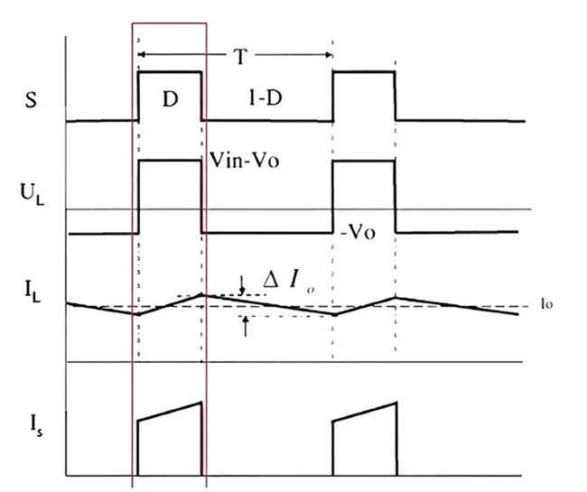
PCB Design Requirements
PCB design for DC-DC converters must carefully address the power path, feedback loop, and thermal management in order to minimize parasitic inductance and noise, thereby ensuring stable and efficient operation. A series of design rules and layout requirements should be followed to guarantee proper and reliable circuit performance.
- Input Capacitor Placement: The input capacitor should be placed as close as possible to the chip’s input (Vin) and power ground (PGND) pins to reduce the effect of parasitic inductance. Since the input current is discontinuous, parasitic inductance can generate noise that may compromise the chip’s voltage tolerance and the normal operation of logic units. Adding vias at the capacitor’s ground terminal helps reduce impedance.
- Power Loop Design: The power loop should be designed as short and wide as possible to minimize loop area and noise radiation. Since the switching node (SW) is the main source of noise, its area should be minimized while ensuring proper current supply, and it should be kept away from sensitive or noise-prone areas. For example, the inductor should be placed close to the SW pin but away from the feedback line, while the output capacitor should be positioned close to the inductor with additional vias at its ground terminal.
- VCC Capacitor Placement: The VCC capacitor should be directly placed between the chip’s VCC pin and signal ground, preferably on the same PCB layer to avoid the use of vias.
- Feedback (FB) Layout: The feedback section is the most sensitive and interference-prone part of the chip and often a source of system instability. Therefore, special care must be taken in the design and layout of this section.
(1).png)
(1).png)